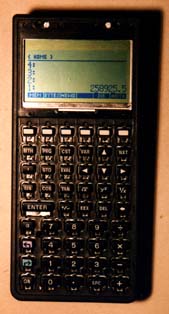
By Djscorpion in Portugal...![]()
SRAMS
32k para 128k e mais
Obrigado por Ter escolhido este site, este site foi feito com muito dificuldade ! foi muitas horas em pesquisa e também algumas experiências que felizmente correu bem , o que vem a seguir são as informações necessárias para fazer um UPGRADE desde 128k até 4 mega ATENÇÃO a partir dos 512k ainda não formam testados, até este momento tenho feito upgrades até 128k , por que o risco de estragar a HP é menor do que os outros upgrades, mesmo assim foi feito com sucesso , a grande dificuldade em fazer estes upgrades é o facto que neste pais tao lindo como é , é difícil encontrar os respectivos SRAM de 128k , felizmente consegui encontrar alguns que são perfeitos para está conversão de memória.
Eu peço imensa desculpa pela informação que segue
a seguir , de ser em inglês, Eu estou trabalhar numa versão
português. ![]()
![]()
Espero que este site ajuda !!! PARA MAIS INFORMAÇÃO DE UPGRADES DE MAIS DO QUE 256K MANDAM UM EMAIL
O meu contacto é DJSCORPION@XOOMMAIL.COM
UPGRADE PARA 128K e 256k
Eu tenho posto algumas das minhas opiniões ao logo desta pagina
This document is based on the file 48GS256K.ZIP. The
original document describe how to upgrade your HP48G(S) to 256K with standard
DIL ram packages. I would like to thanks Thomas Otten and Thijs Kaper
for their initial works.
You can download
the file 48gs256k.zip
In this document, I explain how to use SMD (surface mounted chip)
ram chips to do the same upgrade, but for HP48G only. If you want to upgrade
the HP48S, you should refer to the original file. Moreover, you'll find
some pictures showing how to open your HP without damages, and what
looks like the upgrade.
Parts needed: Não se encontra estes em Portugal , SÓ EQUIVALENTES !!!
You need also a thin soldering iron. The soldering tip should
be less than 2mm (1/10 inch) wide.
You'll need as secondary accessories:
Provide yourself also with a lot of patience! É VERDADE MUITA PACIENCIA!!
The numbers inside brackets are the size of the document with pictures.
Usefull datas:
Disassembling the hp48
Despite the fact that that's pretty scary, I will entail what I know here.
Thanks to David Holmes for taking the first step and helping make my attempt
more informed.
None of the information that follows came from hp, so if what I say starts
to sound rather official, it's not.
For the few folks out there who've actually had to send their hp48 back
to hp for service, you probably ended up with an entirely new unit. I suspect
the reason for this, aside from some labor cost savings on the part of
hp, is that they really aren't much fun to take apart. You can draw your
own conclusions as to why it was designed that way.
You will need to remove the batteries for a while to disassemble the unit, and you may have them out long enough to cause memory loss (although in my case, even 2 days didn't wipe anything out).
Moreover, you will remove the original ram chip! If you manage not to loose the memory, you are not born on this planet!!
The overlay is attached with double- sided tape of some sort. A little care and patience will allow you to remove it only slightly warped, and it is fairly easy to straighten out later. I took a small jewelers screwdriver and started prying near the "ON" button, and worked upward toward the screen.
|
|
When you get near the screen, try to preserve the shape of the overlay
because that portion is a bit more difficult to properly straighten later.
Once the overlay is removed, put it in a container or somewhere away from
dust. The double-sided tape should stay with the overlay (mine did, at
least) and will gather dust and stuff making it less sticky if left out
in the open. 48sx owners will need to remove the little hp logo insert
above the screen as well.
I used a hair dryer to warm a little bit the glue. It's then
easier to remove the overlay. But you must be very carrefull not
to over heat the HP, especially the LCD display!! I placed a cardboard
above the LCD and blew hot hair only in the opposite direction. You will
not manage to heat all the overlay, but at least until the second or third
row of keys it'll be easier! - SG
|
|
|
|
Before |
After |
You can see - under the thin metal overlay you just removed - 10 plastic rivets.You can see on this picture their location.

Believe it or not, these rivets aren't all that critical to holding
the unit together, so you can be as careful or as reckless as you want
(I prefer reckless, because I hate plastic rivets). A good way to carefully
remove the rivet heads is to use a flat head screwdriver that is the same
width as the recessed rivet hole (4mm?) and "drill" the head
away by hand with the screwdriver.
(I used a real drill to do this operation - SG).
|
Drilling the rivets |
|
|
The same operation, but in 2D and black&white! |
|
The head is about 2mm deep, so stop "drilling" there to leave the keyboard material shoulder intact for easier reconnection later. There are 6 rivets near the number keys and four above the screen. These rivets above the screen perform more of a holding function than the others, and you may want to consider using some screws and small washers to replace them when you re-assemble.
 This
is a close-up of a drilled rivet.
This
is a close-up of a drilled rivet.
The upper half of the calculator contains almost all of the components except for the piezo "beeper" element, and there are no interconnecting wires between halves.
The only obstacle is the snap-together "hooks" that David Holmes refers to. These hooks are positioned near the [A], [F], [SIN], [1/x], [ON], [+] and [.] keys (the one by the [.] key is a real bugger!). Refer to the cutaway diagram below for details.
Key overlay here ___
                    \     ____________
                     \   |            |
             ____________|    ______  |
                             |   _  | |  <--- Upper section.
                             |  | | | |
             ________________|  | | |_|
                             |  | |___
  Circuit board and other    |  |     |
  components (affixed to     | /      |  <--- Lower section.
  upper section)             |/__     |        Has a lip which
                             |   |    |        engages with metal
           Metal "hook" --- | / |    |        "hook" from upper
                             |/  |    |        section.
                             |   |    |
             ________________|   |    |
                                 |    |
To separate the two sections, you will need to push the lower section out and down around the hooks. You can't do this from the outside because the upper section hangs over the lower, so you have to go from the inside. Luckily, the six slots in the keyboard (used by the separate user-overlays that fit over the original overlay) near the [MTH], [ENTER], [blushift], [NXT], [backspace] and [-], come in handy for this. These slots are not exactly lined up with the hooks, but are close enough. You can insert something in these holes (I used a jewelers screwdriver, flat head) at an angle that is mostly down and somewhat out, to a depth of about 5mm, and come in contact with the lower section. Push the lower section out about 2mm (this will take a bit of force), while wedging something in the outside gap to separate and hold the sections apart while working on the other hook positions ( a wooden matchstick works). I recommend starting with the [A] or [F] positions first, working down whichever side you started with, then do the other side, and leave the [.] position for later (there is no helpful slot there).
 |
 |
| The two battery contacts which come through the case will need to go back through the case when the sections separate. The upper contact is hooked on a plastic boss, and needs to be freed from it. Just pop it off with your finger or a screwdriver. |
|
(above the screen).
If you have freed all the hooks, the case should sort of hinge at the bottom
edge. This is due to the last hook (near the [.] key). Some careful twisting
and working of the sections should free this hook as well. You should now
be able to completely separate the two sections. I recommend at this point
that you take a pair of pliers and flatten that last hook so that it will
not hold next time. It is really not needed anyway, as the other six hooks
hold the unit together just fine.
Now you can poke around and explore things. Be careful what
you touch, I'm not sure how sensitive the insides are to static discharge
from your fingers, etc.
If you're interested in adding stuff, some open real estate can be found
in the areas between the battery compartment and the card receivers, and
in the cavities in the lower section below the tin shielding on either
side of the card ports (this is where I put some jacks). If you own a 48s,
you may find a lot more space.
If you want to disassemble the unit further, like removing the circuit board from the upper section, you have a considerably tougher job on your hands, and you're on your own. Also, if you separate the screen from it's circuit board, you will disturb the rubber conductors (there are two) which provide electrical connection to the lcd rows and columns (zebra strips). Upon reassembly of the screen, you may find that you have lost some rows or columns in the display (not permanent, just a zebra strip alignment problem) and will have to keep reassembling and perhaps cleaning until it comes out okay. I haven't done this to my hp (yet) but I have done it to other cheap calculators and it wasn't fun.
The ram chip is the original 32k ram. You can see on the left the four pads waiting for the new 128k ram chip! The PCB of the 48G is the same as the 48GX! It differs only in the fact that in the G ther's missing some chips. Especially the 74HC00 (bottom of the picture) used to manage the port 1, and the 74HC174 used for the bank switching mechanism used at port 2.
The Coil is used to generate regulated 5V (for the chips) and +/- 12V (for serial IO) from the 4.5 V delivered by the 3 batteries.The black capacitor maintain the ram while you are removing the batteries. You will also find there a good +5V source.
Port 1 is on the right, port 2 on the left (for the pins that are not the same for the two ports).
The CPU's name is Saturn. A nice processor with 64 bits internal registers, but with a data bus of 4 bits!!!
Ok, now that you have opened your HP, let's start with the upgrade.
| You must desolder the original 32K ram chip. I used a needle
to bent up the pins while I was heating with the soldering iron. As you
can see, the RAM chip is the left one (the LCD display being up and the
battery case down). There is 28 pins to desolder. We don't need this chip
any more, so you can throw it if you want. Once this is done, check the absence of soldering bridges. Put some fresh solder on all the pins (there must be 32 pins, the first 28 used by the old ram, and the last 4 wich were free), it will be easier to solder the new ram. |
 |
|
|
Solder the new ram, 128K x 8bits static SMD. Take care at the
orientation of the ram: The first pin is down near the ROM chip,
near the battery case. There's a dot on the chip near one corner of the
ram locating the pin number 1. It allready works!! Close the HP (see how to do it) replace the batteries and check if the HP turns ON... If it doesn't, then you are in troubles... Reopen your HP, check all your solders, check for soldering bridges, try to bend up the pins to check if they are good soldered,... If you have done it carrefully, there should be no problems. At this point, you have 128K. You may want to stop now, there's no problem. If on the other hand you are brave enough, you can try to do the second part of the upgrade: adding 128k more for a total of 256k! |
You allready have a 128K ram HP. Let's go for 256K!
You have to solder the second chip above the first. Warning:
It's a hard work... Usually, the pins are a little too short to manage
an easy soldering. You have to solder these pins together with the help
of a tiny piece of wire...
All the pins have to be soldered on the first RAM except 3 of
them: You have to bend up pins # 22, 24 and 30. They have to be connected
to some signals present at the place where the card connector is usually
soldered.
Take a look at the layout of the card connector
and also at the pinout of the rams.
The pins 2,21,37,38 and 39 of the card connector are devided for the two
card slots. For all those pins you have to use only the row of pins that
has more distance from the battery case. This is the row for card slot
1.
 pin 22:  connect it to pin 40 of the connector
 pin 24:     "            " 22           "
 pin 30:     "            " 21           "
There's some additionnal connections to do :
Here's the result:  the
same picture at high
resolution (232k)
the
same picture at high
resolution (232k)
Put now some adhesive tape on the metal shield to prevent shortcuts when you'll close the HP. Close the HP, and ready for the first test!
This is covered in the text by Paul Smith. Pay attention to the "plus" battery connector: it has to snap back into its place or you will get a nice shortcut!
Reassembly-
Putting it back together is much easier. You may need to clean up the remains
of the rivet heads so they will easily reinsert into their holes. Make
sure the battery connections align with their respective holes, and snap
the unit together, applying pressure where the six (or seven, if you left
that one near the [.] key alone) hooks are.

You will probably want to hold the case together at the top with one or two of the rivets there. If you can find a wood screw with a flat or thin head, you can screw it into the body of the rivet and let the head hold the upper section surface. You may need a small washer for this. A machine screw will probably work as well, but will strip the plastic easier and not hold as well. I have only one screw holding mine together and it works fine.
You will probably need to re-shape your tin overlay, as it probably
took a beating during removal. I removed the sticky tape from mine, but
it's probably better not to (unless it really wont stick anymore). Put
wax paper over the tape and put the overlay face down on a hard cover book.
Grab a hammer with a smooth and somewhat flat head, and pound away. DONT
pound away on the part that surrounds the screen (beveled part). You can
probably use your fingers and a little massaging to fix that area. With
a little care you can end up with an overlay that looks like new. Press
the overlay in place and hope it sticks. If not, a little rubber cement
wouldn't hurt.
Have fun!
Paul Smith
|
WARNING: |
|||
To test new memory inside the HP48G, press ON, then ON-D to
enter test mode, and after the vertical line(s) apear press the "k"
key (arrow up). After this the display should say "RAM1 OK 128K"
and something like "RAM2 90000". The first "OK" just
stays on my display a very short time. Press "k" again to test
it another time if you missed the message... Leave test with ON-C.
To test the new internal 128K (the previous test was an external port-mem
test only), press ON, ON-D, and then EEX. Now wait for a message stating
"IRAM OK 128K". Leave the test with ON-C. Don't be afraid if
you see a "fail 100" or "fail 180" mesasage at the
end ! This message was already present before you upgraded your calculator,
and as far as i can see the "fail 180" means that both port-1
and port-2 memory are missing, and in the same way "fail 100"
indicates the missing port-2 memory (you only installed port-1). So if
everything is Ok, you should see the "fail 100" message after
doing the upgrade.
To get rid of the "Invalid card data" message, type
PINIT, or just start using the port.
I wish everybody good luck on doing the upgrade !
|
|
|
|
There's now 256K of ram! |
"You know what? I'm happy..." |
                __                  __      __
     Vcc A15 CE2 WE  A13 A8  A9  A11 OE  A10 CE1 D8  D7  D6  D5  D4
  ____I___I___I___I___I___I___I___I___I___I___I___I___I___I___I___I____
  I  32  31  30  29  28  27  26  25  24  23  22  21  20  19  18  17   I
  I                                                                   I
   \                                                                  I
    I                                                                 I
   /                                                                  I
  I   1   2   3   4   5   6   7   8   9  10  11  12  13  14  15  16   I
  I---I---I---I---I---I---I---I---I---I---I---I---I---I---I---I---I---I
     NC  A16 A14 A12 A7  A6  A5  A4  A3  A2  A1  A0  D1  D2  D3  Gnd
And this is for the built in 32K chip. In my G it's labeled M5M5256BFP and is located just above the battery case (the left one of the two chips located there before you inserted the HC00).
                 __                  __      __
             VCC WE  A13 A8  A9  A11 OE  A10 CE1 D8  D7  D6  D5  D4
           ___I___I___I___I___I___I___I___I___I___I___I___I___I___I____
           I  28  27  26  25  24  23  22  21  20  19  18  17  16  15  I
           I                                                          I
            \                                                         I
             I                                                        I
            /                                                         I
           I   1   2   3   4   5   6   7   8   9  10  11  12  13  14  I
           I- -I---I---I---I---I---I---I---I---I---I---I---I---I---I--I
              A14 A12 A7  A6  A5  A4  A3  A2  A1  A0  D1  D2  D3  Gnd
As you can see the layout is nearly the same. Not for the pin numbers
but for the pin places if the chips are right assigned.
Be sure to isolate everything. I glued some paper to the back side of the
RAM chips to keep it away from the shielding. A little sheet of paper between
pin 20 of the 32K and it's former connection keeps these pins apart.
This chip can be used if you want to add more than 256k to your HP48G(X).
Here is the 512k ram pinout:
         |-------\_/-------|
         |                 |
   A18 - | 1            32 | - Vcc
   A16 - | 2            31 | - A15
   A14 - | 3            30 | - A17
   A12 - | 4            29 | - Negative WE
    A7 - | 5            28 | - A13
    A6 - | 6            27 | - A8
    A5 - | 7            26 | - A9
    A4 - | 8            25 | - A11
    A3 - | 9            24 | - Negative OE
    A2 - | 10           23 | - A10
    A1 - | 11           22 | - Negative CS
    A0 - | 12           21 | - D7
    D0 - | 13           20 | - D6
    D1 - | 14           19 | - D5
    D2 - | 15           18 | - D4
   VSS - | 16           17 | - D3
         |                 |
         |-----------------|
(Taken from the file 48GS256K.ZIP)
If you have a look on the circuit board you will see a row of pins that
connect to the chip card slots of the 48GX. Most pins are connected in
the G, too. If the battery case points to you the pins are numbered RIGHT
TO LEFT. You can verify that if you know that the pins 2,21,37,38 and 39
are devided for the two card slots. These are the pins.
PIN:   Signal:                    PIN:   Signal:
1      VCC (only if HP48 is ON)   21     Card enable (active HIGH)
2      RAM Battery measure        22     Output enable (active low)
3      Addr. 0                    23     Data 1
4      Addr. 1                    24     Data 2
5      Addr. 2                    25     Data 3
6      Addr. 3                    26     Data 4
7      Addr. 4                    27     Data 5
8      Addr. 5                    28     Data 6
9      Addr. 6                    29     Data 7
10     Addr. 7                    30     Data 8
11     Addr. 8                    31     Video (port1) / EA 0
12     Addr. 9                    32     Video (port1) / EA 1
13     Addr. 10                   33     Video (port1) / EA 2
14     Addr. 11                   34     Video (port1) / EA 3
15     Addr. 12                   35     Video (port1) / EA 4
16     Addr. 13                   36     Video (port1) / EA 5
17     Addr. 14                   37     Write prot. in (act low)
18     Addr. 15                   38     Card present in (act high)
19     Addr. 16                   39     Card type (low for RAM)
20     Write enable (active low)  40     Ground
Notes:
1. In the G the pins 31 to 36 (Extended Adress pins) are connected to an
empty chip place on the board. They are needed to address the larger RAM
cards (up to 4MB) and provide additional card enable signals. Carl Raffa
told me there is a HC174 in the GX but if you don't plan to connect a RAM
expansion box to your 48 or have really small RAM chips you don't need
it. The G with ROM version K will not be able to use that at all since
the command PINIT is missing in that release (thanks to James H. Cloos,
Jr. for that info).
2. Pin 22 leads to a second empty chip place (on the right side above the
battery case). Thanks to Carl Raffa I now know that this place has to be
filled with an 74HC00 (costs ca. 50 cents) to decode the OE (output enable)
pin for simulating a RAM card in the 48G.
I thank these gugs for this upgrade to be possible without these pictures this good be quite worse!!
Agradeço muito a estes pessoas que tornaram este upgrade possível foi com esta informação que eu consegui fazer o upgrade ao meu e outros !!!
O MEU CONTACTO NOVAMENTO PARA UPGRADES E INFORMAÇÃO É
EMAIL : DJSCORPION@XOOMMAILL.COM
CABOS DE LIGAÇÃO
DE
HP PARA PC

COMO FAZER UM CABO SERIAL PARA HP48G ou GX
Você de ter tido a mesma sensação de alívio quando encontrou programas na Internet para a HP48. Mas o grande problema não é baixar os ditos programinhas, mas sim ter o cabo serial para conectá-la ao computador.
Abaixo mostro como fazer um cabo serial Antes de mais nada, faça uma busca em sua cidade às lojas de informática a procura de cabos de mouse. Não tenha vergonha, peça para desmontar o mouse e ver se o conector que está lá dentro serve na calculadora (leve ela junto, se for o caso). Não esqueça também de ver se eles tem um adaptador 9 pin para 25 pin serial. Essa peça normalmente eles querem verder para você (tenha cuidado, o preço varia muito de uma loja para outra). Tá, mas chega de papo e vamos por a mão na massa.
MATERIAL NECESSÁRIO:
* Um cabo de mouse;
* Um adaptador 9 pin para 25 pin; * Chave de fenda pequena (aquelas do Paraguai serve); * Alicate; * Fita isolante; * Muita paciência.
COMO MONTAR:
* Abra o mouse e tire o cabinho da placa dele;
* Corte o fio na extremidade do plug; * Desencape o cabo. Dentro dele tem 4 fios (algumas aberrações de mice tem 5). Descasque aproximadamente 3cm cada um; * Coloque o plugzinho na calculadora. Deixe-a de costas para você de modos que o desenho do manual fique igual ao que você está vendo; * Enrrole cada um dos fios descascados da chavezinha de fenda; * Observe então o fio da esquerda deve ser ligado no pino número 1; * Ligue o que está ao lado do fio da esquerda ao pino número 2; * Ligue o que está ao lado do fio da direita ao pino número 3; * E o fio que está na direita ao pino número 5; * Use a fita isolante para fixar os fios nos pinos. Passe por cima primeiro e depois pelos lados. Os adaptadores 9 pin para 25 pin normalmente trazem impressos os números dos pinos, mas se o seu não tiver é fácil descobrir. Segure o adaptador e deixe a parte que tiver mais pininhos para cima. O pino que estiver a sua direita é o número o um. O que estiver ao seu lado é o dois ao lado do dois está o três e assim por diante.
Copyright© Leonardo Rosa Silva Barbosa
Obrigado Leonardo de Djscorpion
Electronic mail address
DJSCORPION@XOOMMAIL.COM
Please send me mail telling me what you think about this page and how I might improve it.
| http://mercury.beseen.com/guestbook/d/38765/sign.html">Sign GuestBook | src="http://www.beseen.com/images/beseenbutton.gif" height=31 width=88 alt="Beseen.com"> |


